Τρίτη 10 Σεπτεμβρίου 2013

Semiconductor materials and Fermi Levels

Fermi Level

The Fermi Level is the equilibrium electrochemical potential. It represents the expected value  of the change in energy of one electron added to (or taken from) the system. For any state with Energy E, the probability of occupation for that state is given by the Fermi-Dirac distribution:
$$ f_{FD}(E)=\frac{1}{1+exp\left ( \frac{E-E_{f}}{kT} \right )} $$
The Fermi level represents the boundary between the mostly filled and mostly empty states in equilibrium, with temperature determining how sharp that boundary is. Far above or below the Fermi level, the Fermi-Dirac distribution can be approximated by the Boltzmann distribution:
$$ f_{FD}(E)\cong \begin{cases}
exp(E-\frac{E_{f}}{kT}) & \text{, if } E>E_{f}+3kT \\
1-exp(E_{f}-\frac{E}{kT}) & \text{, if } E<E_{f}-3kT
\end{cases} $$
To calculate the relation between Fermi level and carrier concentration, it is necessary to specify the density of states in the conduction (or valence) band. For a single parabolic conduction band with:
$$ E=E_{c}+ \frac{\hbar^2k_{x}^{2}}{2m_{x}^{*}}+\frac{\hbar^2k_{y}^{2}}{2m_{y}^{*}}+\frac{\hbar^2k_{z}^{2}}{2m_{z}^{*}} $$ the density of states is: 
$$ N(E)=\frac{\sqrt{m_{z}^{*}m_{y}^{*}m_{x}^{*}}}{2\pi^{2}}\left ( \frac{2}{\hbar} \right )^{3/2} \sqrt{E-E_{c}} $$
For a semiconductor with multiple band externa (for example Si with 6 equivalent conduction band minima and 2 nonequivalent valence band maxima), the density of states for all the bands must be added together.  The result is:
$$ N(E)=\frac{1}{2\pi^{2}}\left ( \frac{2m_{dn}}{\hbar} \right )^{3/2}\sqrt{E-E_{c}} $$, where mdn is the density-of-states effective mass for the conduction band.
The number of electrons in the conduction band is given by integrating the Fermi-Dirac distribution times the density of states over energy.
$$ n=\int_{0}^{\infty }f_{FD}(E)N(E)dE = N_{c}F_{1/2}\left ( \frac{E_{f}-E_{c}}{kT} \right )  $$, where $$ N_{c}=2\left ( \frac{m_{dn}kT}{2\pi \hbar^{2}} \right ),\; \; \;  F_{n}(\eta )=\frac{2}{\sqrt{\pi}}\int_{0}^{\infty }\frac{x^{n}dn}{1+exp(x-\eta )} $$
Similarly for the valence band,
$$ p=\int_{0}^{\infty }f_{FD}(E)N(E)dE = N_{v}F_{1/2}\left ( \frac{E_{v}-E_{f}}{kT} \right )  $$

Equilibrium electrochemical potential:

Considering a non-degenerate material for simplicity, the Fermi level can be written in terms of the electron concentration:
$$ E_{f}=E_{c}+kTln\left ( \frac{n}{N_{c}} \right )=E_{i}+kTln\left ( \frac{n}{n_{i}} \right ) $$
The electric field is defined as the negative gradient of the electrical potential ψ, but it can also be expressed in termos of the gradient in the conduction or valence band (no change in bandgap).
$$ \varepsilon\equiv -\frac{d\psi }{dx}=\frac{1}{q}\frac{dE_{c}}{dx}=\frac{1}{q}\frac{dE_{v}}{dx}=\frac{1}{q}\frac{dE_{i}}{dx} $$
If we apply these equations plus the Einstein relationsn/q=Dn/kT) to the electron current equation, it is possible to show that:
$$ J_{n}=n\mu_{n}\frac{dE_{f}}{dx} $$
Thus in equilibrium,  Jn = 0, Ef = constant. Another way to think about this fact is that if there was a change in electron potential with position, electrons could move around to reduce the energy of the system.

Quasi-Fermi Levels

Under thermal equilibrium, we use the equations relation the Fermi level to the electron and hole concentrations. For example,
$$ n=n_{i}exp\left ( \frac{E_{f}-E_{i}}{kT} \right ) $$
However, if we have injection (np>ni2) or extraction (np<ni2), then we are not in equilibrium and therefore cannot use these relationships, because Ef is no longer meaningful.
To replace Ef, we define two new quantities called quasi-Fermi levels:
$$ n=n_{i}exp\left ( \frac{E_{fn}-E_{i}}{kT} \right )=N_{c}exp\left ( -\frac{E_{c}-E_{fn}}{kt} \right ) $$
where Efn is the quasi-Fermi level for electrons, while for holes:
$$ p=n_{i}exp\left ( \frac{E_{i}-E_{fp}}{kT} \right )=N_{v}exp\left ( -\frac{E_{fp}-E_{v}}{kt} \right ) $$
The quasi-Fermi levels are mathematical tools and their values are chosen so that we can extend our familiar equilibrium equations to nonequilibrium situations (even for degenerate statistics). Out of equilibrium, Efn ≠ Efp and |Efn - Efp| is a measure of how far removed the semiconductor is from equilibrium.
$$ pn=n_{i}^{2}exp\left ( \frac{E_{fn}-E_{fp}}{kt} \right ) $$
In addition, the gradients in the quasi-Fermi levels are the dividing forces for carrier fluxes. Thus, as for Ef in equilibrium:
$$ J_{n}=n \mu_{n}\frac{dE_{fn}}{dx},\; \; J_{p}=-p \mu_{p}\frac{dE_{fp}}{dx} $$


Δευτέρα 9 Σεπτεμβρίου 2013

Power Amplifier Differential Input Stage Testing


Most of the power amplifiers in the wild today are based about the three stage achitecture proposed by Mr. Lin or RCA in 1950. Three stage architecture, increases freedom of design, separates distortion sources and allows a more stable (in terms of Nyquist stability) and linear amplifier to be designed.
The basic three stage architecture is depicted in Fig.1.
Fig.1 Lin three stage architecture
Lets remember some basic principles of power amplifiers of this architecture. 
First lets talk about the function of each stage:
  • The input stage is a transcundactance stage (Long Tailed Pair LTP): voltage difference in, current out
  • VAS stage is a transadmittance stage: current in, voltage out
  • Output stage (drivers and output semiconductors): unity gain voltage follower (voltage amplifier)
Second, we seperate the spectrum range in to two ranges; the LF range and the HF range, which are seperated by the dominant pole P1 created by the CC Miller compensation capacitor at the VAS stage.
The amplifier's Open-Loop Gain for LF is: $$ A_{O(LF)}=g_{m}\cdot \beta_{VAS} \cdot Z_{c} $$
where gm is the transconductace of the input stage, β is the beta parameter of the VAS BJT transostor and Zc is the impendance of the load at the collector of the VAS stage. Notice that the gain remains constant for frequencies below the dominant pole P1.
For HF: $$ A_{O(HF)}=\frac{g_{m}}{2\pi fC_{c}} $$, where f is the frequency and Cc is the capacitance of the Miller compensation capacitor of the VAS.

Today I ran some simulation experiments, focusing on the differential input stage of the amplifier.
How do we separate the input stage for testing? I stumbled across two ingenious methods proposed by Douglas Self and Randy Slone and today I employed the method of the latter to test input stage, as seen in Fig.2, which contains a very basic input stage topology, a buffered VAS stage with a constant current source as VAS collector load. Containing the VAS stage in the method is essential, because of the NFB required to be given to the Q2 of the differential input stage. Output stage is not needed. (For further details look Randy Slone: High Power Audio Amplifier Design Handbook).
Fig.2 Input stage separation (method by Randy Slone)

The transconductance and linearity of the input stage is a function of the tail current of the LTP and how balanced is it between the two legs in the collectors of Q1, Q2 in Fig.2.
R1 , R6, R7, Q1, Q2 form the input stage, R3, R4, R5, C4, C5, D1 is the NFB decoupling network, R2, C2, C3 the input decoupling network, C1, C7 the power supply decoupling capacitors, R8, C6, Q3, Q4, I1 form the VAS stage.

The current balance and regulation of the input stage is bad. The  DC current balance when no signal is present 0.19mA run through Q1, whereas at Q2 there is 3.89mA. Very bad!!!!
A signal of 2.115Vpk is applied at the input to produce an output at about ~94.2Vpk-pk close to the clipping level. The AC current that flows in Q1, Q2 is shown in Fig.3 and shows a great imbalance that gives a rise in harmonic distortion, especially in second and third harmonics.
Fig.3a Current imbalance at simple input stage Fig.3b Transconductance (rms) of simple input stage
The second harmonic rise is due to the absence of current regulation in the emitters of Q1 and Q2, but the third harmonic rise is due to current imbalance between Q1 and Q2 collector legs.
Improving the circuit demands adding a current source as a form of emitter degeneration and a current mirror as collector load that fixes the imbalance.
Fig.4 Proper fixes for input stage linearity
Q5, Q6, R1, R9, R10, R11, C8 are the current source for the emitters of the LTP. Q7, Q8, R6, R7 are the current mirror for the collectors of the LTP. Current source guarantees a constant current regulation independent of the LTP impedance, while current mirror fixes the current imbalance between Q1 and Q2 collector legs. R6 and R7 are current mirror's degeneration resistors for eleminating the effect of β of Q7, Q8 (because they will not be exactly the same). Any change in current in Q7 will be reflected in Q8 and vice versa, thus keeping a balance.
R1 is the degeneration resistor for Q5, increasing linearity of current source and C8 is required for Power Supply Rejection at the current source.
The DC currents at Q1 and Q2 when no signal is present are: 2.23mA for Q1 and 2.26mA for Q2. Great improvement!!!
A transient analysis for the same input signal as before is shown in Fig.5.
Fig.5a Current balance at fixed input stage Fig.5b Transconductance (rms) of fixed input stage
 We see the balance in the AC current at Q1, Q2 and the transconductance being 100 times greater than the simple imput stage. In Fig.6a and Fig.6b the harmonic content for simple and fixed input stages is shown for an input signal at 15kHz.
Fig.6a Harmonics @15kHz for Simple Input Stage Fig.6b Harmonics @15kHz for Fixed Input Stage


Κυριακή 8 Σεπτεμβρίου 2013

Boosting power supply available current

I just finished constructing an adjustable Power Supply Unit (PSU) using the common and highly-available LM317 regulator. I intended to use this supply to power light loads, such as stomp boxes and small audio effect units. Of course, a moment had come, when I needed to power a heavier load; a small power amplifier I designed. The PSU I created could not drive that demanding load  and I had to reconstruct the circuit of the supply.

This time I added a current booster circuit using the TIP32C transistor with the LM317 regulator to be able to drive heavy loads. The transformer is not shown in the schematics, only its output that is 12VAC.

In Fig.1 the original power supply circuit is showed (without current booster).

Fig.1 LM317 adjustable power supply with 100kΩ load
Using a load of 100kΩ all things run nice and we get the following output (Fig.2)
Fig.2 DC output voltage with 100kΩ load
Now, if we decrease the value of the load resistor - making a heavier and current demanding load - we get the following graph (Fig.3).
Fig.3 DC output voltage with 4Ω load
We see that the output voltage sagged (dropped) to about 8VDC, indicating that the power supply cannot supply this heavy load the current it requires.

The current boosted Power Supply I designed is seen in Fig.4.
Fig.4 Adjustable Power Supply with current booster using TIP32C
The concept is that when the LM317 comes to its limits, the TIP32C power transistor is turned on to supply extra current to the load in parallel with the LM317. Of course I used 4 TIP32C in parallel to increase the current boost available. The power transistors turn on when there is enough voltage drop across resistor R1 to overcome their base emitter voltage Vbe. (Such voltage drop in the R1 means that the LM317 has come to its limits and the power supply unit starts sagging).

In Fig.5 a plot is seen for a heavy load of 4Ω.
Fig.5 DC output voltage for current boosted power supply
We seen now that the power supply does not sag. Instead to delivers the required current to the 4Ω load, maintaining the required output voltage at ~12VDC and delivering ~12/VDC/4Ω = ~3Α current.

The ripple voltage of the output is at about ~1V which is acceptable enough, because it is below the standard 10% limit and will not become a noise figure for amplifiers having high enough Power Supply Rejection Ratio PSRR (99% of the available solid state amplifiers). Of course the ripple can be further reduced and the simplest method to do that is to enlarge the reservoir capacitor C1. Increasing it though, the inrush current sucked by the MAINS will be increased, unless a soft-start circuit or a suitable trasformer (saturation limit, windings, etc) is placed. In Fig.6 a plot for a larger C1 is shown. Increasing C1 to 22000μF decreases ripple current to about ~0.5V.
Fig.6 Current boosted power supply with larger reservoir capacitor

Fig.7 Input current requirement for current boosted power supply

The power dissipated in the load is about 12VDC*3A = 36W. The input current for the power supply required to drive such a load is sen in Fig.7 (with C1=10000μF). The rms current is at about 5A, with peaks at about 12.5A. That means if you have a fast MAINS fuse it will turn off. 12VAC*5A = 60W power is required from the transformer before the circuit shown here.  Of course the transformer will worsen the things a little bit. 60W for 36W is the prise we pay for a very simple linear power supply circuit. There are many methods for increasing power supply efficiency, but this is not the purpose of this power supply, since it is a test equipment.


Negative Feedback & Total Harmonic Distortion (THD) of Class B Push-Pull

This is a continuation of this post.

Below is a table describing the results of Fourier Analysis up to the 15th harmonic and the Total Harmonic Distortion (THD) at 1kHz frequency for circuits with no NFB or with NFB and different types of OpAmps as the differential input stage. With no Negative Feedback applied, the crossover distortion rises the THD to  about 20%. Applying a simple feedback network with an opamp as a differential input stage the THD drops below 0.1% and with NE5534 precision opamp it goes further down to 0.00019% a very acceptable level. We see, that we can decrease THD at very low level, even without a sophisticated bias network or other linearizing sub-circuits.
With LM741H or TL072, the THD has dropped and the odd harmonics play a dominant role in the harmonic content. On the other hand, NE5534 decreases the whole harmonic content very much, with even harmonics having a greater share this time.

Description Fourier Analysis THD @1kHz
No NFB
20.019%
NFB with LM741H General Purpose OpAmp
0.0789107%
NFB with TL072CP JFET-Input OpAmp
0.0231932%
NFB with NE5532 Low Noise Audio OpAmp
0.00794657%
NFB with NE5534 Low Noise Audio OpAmp
0.000198106%

How Negative Feedback eliminates crossover distortion

First, listen to the following .wav files to hear the difference of an audio signal played through an amplifier with crossover-distortion and another one played through a negative feedback linearized amplifier.

1. Linearized (Negative Feedback): Piano
2. Crossover distortion (no Negative Feedback): Piano

3. Linearized (Negative Feedback): Beethoven's 9th Symphony, Part I
4. Crossover distortion (no Negative Feedback): Beethoven's 9th Symphony, Part I

Hear the difference? Very annoying and unpleasing the sound of crossover distortion. Amongst audiophiles, low amounts of crossover distortion is far worse than large amounts of audio clipping.
(If you are not interested in electronics, go to the end of the post where crest factor is explained.)

(Note: output .wav files were produced through an LTSpice amplifier circuit. This experiment alone, proves the consistency of basic negative feedback theory.)

Now, we will see how negative feedback efficiently works to linearize non-linear components in the forward path of a signal and especially how it decreases the crossover distortion of an amplifier.
Consider a Class B push-pull amplifier output stage with complementary NPN/PNP transistors used in emitter-follower configuration (Fig. 1).

Fig.1 Basic class B amplifier
 We know that all transistors have an inherent turn-on base-emitter voltage Vbe, that need to be overpassed in order the transistor to come into the active region of its operation. Working in a Class B topology, this Vbe, causes a problem; a dead-zone when the input signal is smaller that Vbe and thus not amplified because transistors are in their cutoff region. Of course this causes distortion in the output signal, the so called crossover-distortion (because it occurs when the signal crosses the x-axis in the time domain), which is very audible and annoying and huge efforts are given to eliminate it in audiophile amplifiers. Fig.2 shows the simulation of the output of the amplifier  for 1kHz sine-wave at 1Vrms.

Fig.2 Crossover distortion in Class B amplifier
Notice the dead-zone that occurs at around 0 μsec, 500 μsec ανδ 1 μsec and its duration is the time the sine wave spends below Vbe (NPN) or -Vbe (PNP).

Consider now the topology in seen in Fig.3, enhanced with a differential input stage and global negative feedback.
Fig.3 Class B with NFB
In Fig.4 is the simulation of the output. We see that there is no crossover distortion in the output waveform and that is because the global negative feedback worked to linearize the output in order to accurately follow the input signal (basic feedback theory).
Fig.4 Output of the amplifier with NFB
This does not mean that the turn-on voltage of the transistors (the dead-zone) is gone, but the negative feedback with the differential input stage created an error signal at point in2 in Fig.3, which has such a shape to customize the output. Lets see in Fig.5 what is the waveform of the output of the input stage (in2). We can metaphorically say the error signal is the complementary of the open-loop output signal (with no negative feedback) and when they sum they create the linearized output that is an amplified version of the input.
Fig.5 Output of the differential input stage.
Combining error, open-loop output and closed-loop output signals we get the plot at Fig.6.


Fig.6 Combined plot


Coming back to the music (.wav files in top of this post), we see that cross-over distortion has a larger effect on signals that are of low amplitude, because they spend most time in the transistors dead-zone. So, listening to piece of classical music for example, which has a lot of dynamics in playing (many low passages, etc), very little amount of crossover distortion can ruin the whole listening experience. The song parts that are low in amplitude (pianissimo) are never heard, because they are in the dead-zone and silence has taken their place. In Fig.7 and Fig.8 the two waveforms of a part of Beethoven's 9th Symphony are compared. The former being the output of a circuit with negative feedback and thus no crossover distortion and the latter the output of a circuit with crossover distortion.

Fig.7 No crossover distortion
Fig.8 Crossover distortion
Notice the low passages of the musical piece as seen in Fig.7; they are disappeared in Fig.8 and almost silence has taken their place. In practice it will be even worse; there will be no silence in their place but noise, thus affecting the SNR ratio of the whole waveform. In Fig.7, noise is overpassed by the signal (greater SNR ratio). On the other hand, listening to a song that is compressed to be as loud as possible (low dynamics), less information is lost, because the signal spends most time in the active region of the transistors (close to saturation). Thus, the missing of information because of the crossover distortion is determined by the crest factor of the waveform of the audio recording. Crest factor is the ratio of peak values to the rms value of amplitude of the waveform.
$$ C=\frac{|V|_{peak}}{V_{rms}} $$


Τρίτη 27 Αυγούστου 2013

Negative Feedback and Stability in Amplifiers


In this section I assume you already know the basic principles of negative feedback and how it is used in operational amplifiers (OpAmps) and amplifiers in general. Audio amplifiers, especially power amplifiers, employ the principle of global negative feedback, where portion of the output is fed back into the input stage of the amplifier and compared with the input signal, in order to increase linearity and frequency response of the amplifier. This principle is commonly used in OpAmps, where the user utilizes negative feedback (It is not employed inside the chip), and it is the same with discrete audio power amplifiers.

In Fig. 1 a generic opamp is depicted with a feedback network (β), which feeds back β portion of the output.
Fig.1 Generic amplifier with NFB
The loop gain is: 
$$ A_{loop}=A_{o} \cdot \beta $$
where Ao is the open loop gain of the amplifier and β is the portion of the output fed back to the input.
The output voltage is then:
$$ V_{out}=V_{in}\cdot \frac{A_{o}}{1+A_{o}\cdot \beta } $$
The feedback network and the amplifier itself consists of several components, which can introduce a delay in the signal, a phase-shift. (Remember that a simple RC low-pass filter for example introduces a 90 degree phase shift in the output voltage for frequencies above the cutoff (-3dB) frequency.)
If there is enough such delay to produce a 180 degree phase shift and the loop gain of the amplifier is greater or equal to unity (Av >= 1), then there will be positive feedback and the fed back signal will add to the input, resulting in oscillation of the amplifier.
(In modern electronics there is a term which is called phase margin: the difference of the actual phase shift and 180 degrees. In the presence of negative feedback a phase margin of 0 degrees at a frequency where loop gain is equal or greater to 1 leads to instability.
The lower safety limit for phase margin is 45 degrees. For example if at a signal frequency f the loop gain  is 1 and phase margin is below 45 degrees, it will lead to amplifier instability.)

The open loop bode plot of an opamp is depicted in Plot 1, where there is a pole frequency p1
after which gain decreases with 20db/decade rate. The vast majory of opamps in the market have a plot like this.

Plot 1. Open loop bode plot


The bode plot of an ideal negative feedback network is shown in Plot 2, where there are no poles and no phase shift.

Plot 2. Negative feedback bode plot

Combining the open loop and the negative feedback plots we get the loop gain bode plot of the amplifier as shown in Plot 3.

Plot 3. Loop gain bode plot


Pole p1 introduces a 90 degree phase shift and gain reduces by 20db/decade. At the crossing point of 0dB the slope is 20dB/decade which is ok for the stability of the amplifier.

Now, lets assume that there is some parasitic capacitance in the feedback network which creates a bode plot seen in Plot 4. Pole p1 introduces a 90 degree phase shift in β and a 20dB/decade decrease rate.
Plot 4. Negative feedback with capacitance
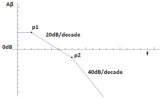
Now, combining the open loop bode plot with the negative feedback plot we have the following plot (Plot 5).
Plot 5. Loop gain bode plot with capacitance in the negative feedback network

The capacitance which created a pole in the feedback network, introduced a second pole p2 in the loop gain bode plot. Pole p1 introduced 90 degree phase shift and ploe p2 another 90 degree phase shift. After p2 the slope is 40dB/decade. As p2 is above the 0dB crossing point, the slope is 40dB/decade at 0dB, meaning that enough phase shift is acquired to make the system probably unstable.

 In general we do not want the slope of the plot to be above 20db/decade at the crossing point (where gain is unity).

 Lets consider the use of an opamp in a non-inverting configuration as a voltage follower in Fig. 2.

Fig.2 Voltage follower
Being a voltage follower we know that the loop gain is equal to the open loop gain:
$$ A_{o}=A_{o} \cdot \beta $$
because β = 1.

The vast majority of the opamps in the market have an open loop gain bode plot as in Plot 1, where the slope is 20db/decade at the 0dB crossing point. Because β=1, the loop gain bode plot will be the same as the open loop gain bode plot and the amplifier is stable.
Nevertheless, there are some opamps out there which have an open loop bode plot like Plot 6.
Plot 6. Open loop gain bode plot of a market opamp
Because β = 1, the loop gain bode plot will be the same. We see that two poles (p1, p2) exist above the 0dB line, so the slope after p2 is 40dB/decade, resulting in an unstable amplifier.


So, what do we do to bring the amplifier in a stable situation?
One solution is to bring the pole p2 under the 0dB line, in order the slope to be 20dB/decade at the 0dB line. To do these we must add a voltage divider network in the feedack loop to reduce β, as seen in Fig. 3. In this case β = 1/10.
Of course the price to pay is that the closed loop gain of the amplifier is increased and is not more a true voltage follower.
Fig 3. Negative feedback with voltage devider
The result, will be a plot similar to Plot 6, but decreased in magnitude, so pole p2 is below 0dB and the slope at the 0dB crossing point is 20dB/decade (Plot 7).
Plot 7. Loop gain bode plot for stable amplifier
After p1 the slope is 20dB/decade, reaching pole p2 after which the slope is 40dB/decade, but does not concern us because the loop gain at that point is below 0dB (unity) and cannot result in oscillation.


Σάββατο 3 Μαρτίου 2012

Designing low noise small-signal attenuators

It seems one of the trivial things to do, creating an attenuator with passive components.
If we want to attenuate the signal by 6dB, then what is more easy, than putting two equal value resistors
in series and form a voltage divider.
But that is that the truth? Equal value yes, but with what value?

Fig.1 shows a classic voltage divider used to attenuate a signal.


Let as consider now how the signal flows.

The signal comes from a source that has an output impedance and the lowest output impedance you will encounter in professional audio equipment is not smaller that 50Ω.  So, the Johnson noise created is -135.2dBu, a low limit.

The maximum signal an OpAmp can handle is +22dBu, as a result the maximum dynamic range is:
135.2+22 = 155.2dB. The dynamic range of the ear is about 130dB.

Let us now examine the circuit with different resistor values. They cannot be low, because they will overload the previous circuit, causing distortion and reduced headroom and the cannot be too high because the induce large Johnson noise. So what is the optimum solution?


If we use 1kΩ resistors, then the Johnson noise floor becomes -125.2dB, because the effective resistor value for two 1k parallel resistor is 500Ω as seen from the output. The input impedance as seen from the source is 2kΩ.
We just raised noise by 10dB and probably the next components in the signal chain will further raise this noise more.

Now, the standard input impedance for a good audio equipment is at least 10kΩ. It means we will have to use 5k resistors, output impedance 2.5k and this produces a Johnson noise of -118.2dBu.

Of course in most, cases resistors near 100k are used because 10k input impedance is not high enough.
For a 100k input impedance we use two 50k resistors with Johnson noise -108.2. That is 27dB more noise than when the signal arrived with -135.2dBu from a 50Ω source.


If we have to use large resistors to create 100k input impedance and even higher, what is the solution to avoid excessive noise contamination?
The solution is to buffer the voltage divider circuit using a good low-noise OpAmp in front of it that can drive heavy loads as shown in Fig.2. OpAmps in general have very high input impedance.
If we use an OpAmp like the low-noise NE5532 we can achieve high input impedance and low noise contamination. The noise produced by NE5532 at its output is -119dBu and we can use two 500 Ω resistors that can be handled by NE5532 as a load. The Johnson noise from those resistors is -128.2dbU.
The output noise of the OpAmp is attenuated just like the normal signal and the result is the half of -119dBu = -125dBu, so the total noise is the sum of noises -128.2dBu and -125dBu, which is -123.3dBu.

Remember that the 6dB attenuator (voltage divider with equal value resistors) is the worst case, since it presents the largest output impedance.


 Table.1 Johnson noise for different voltage dividers, at 25oC
and 22kHz bandwidth.